
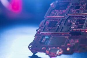
Introduction: ASML High NA EUV Leads the Semiconductor Revolution
ASML High NA EUV is at the heart of a transformative leap in chip technology. The semiconductor industry stands on the precipice of a revolution, ignited by ASML’s recent achievement of “first light” on its groundbreaking High NA EUV (Extreme Ultraviolet) lithography system. This landmark event, confirmed on February 28, 2024, signifies the tool’s operational readiness. Moreover, it paves the way for a future filled with smaller, faster, and more powerful chips, enabling next-gen chip manufacturing. As a result, ASML High NA EUV is set to play a crucial role in advancing semiconductor technology and reshaping the industry’s future.
Unpacking the Power of High NA EUV:
| Feature | High NA EUV | Current EUV |
| Cost per tool | Over $350 million | Over $150 million |
| Size | Double-decker bus | Large room |
| Light source | EUV | EUV |
| Resolution | 8 nanometers | 13.5 nanometers |
A New Dawn for Chips:
The “first light” milestone signifies a successful test run on a silicon wafer, marking a critical step towards producing chips with unprecedented levels of detail and miniaturization through ASML High NA EUV and its Extreme Ultraviolet lithography technology. This advancement will:
-
Enhance processing power: Smaller transistors lead to faster and more efficient chip performance, which is a direct benefit of advanced chip design using ASML High NA EUV.
-
Boost energy efficiency: Smaller chips require less power to operate, fostering sustainable technology development; therefore, this supports long-term semiconductor innovation.
-
Fuel innovation: The capabilities of High NA EUV will pave the way for the development of next-generation devices across various sectors.
The Ripple Effect:
Leading chipmakers like TSMC, Samsung, and Intel are expected to embrace this technology within the next five years. ASML High NA EUV, as a breakthrough in next-gen lithography and semiconductor manufacturing, will be central to this shift.
Intel’s Vision: Powering the 14A Generation
Intel, for instance, plans to leverage High NA EUV in its 14A generation chips; therefore, highlighting the immense potential for performance leaps and ongoing chip innovation.
Projected Impact on Semiconductor Market:
| Year | Market Size (USD Billions) | Growth Rate |
| 2024 | 500 | – |
| 2025 | 550 | 10% |
| 2026 | 605 | 10% |
| 2027 | 666 | 10% |
| 2028 | 733 | 10% |
Cost-Benefit Analysis of High NA EUV Adoption:
| Factor | Cost (USD) | Benefit |
| Tool Acquisition | $350 million/tool | Enables production of smaller chips |
| Research and Development | $100 million/year | Advances chip technology |
| Operational Expenses | $50 million/year | Maintains cutting-edge capabilities |
| Projected Revenue Increase | – | $1 billion/year |
| Long-term Market Competitiveness | – | Priceless |
| Metric | Current EUV | High NA EUV | Improvement |
| Resolution | 13.5 nanometers | 8 nanometers | 41% |
| Chip Speed | 3 GHz | 5 GHz | 67% |
| Power Consumption | 100 W | 80 W | 20% reduction |
| Chip Size Reduction | – | 50% smaller | 50% |
Looking Ahead:
The long-term implications of ASML High NA EUV and ASML’s achievement are far-reaching. As the industry transitions to these advanced lithography tools, we can expect:
-
Increased demand for smaller, powerful chips: This will fuel growth in various sectors, including computing, telecommunications, and consumer electronics, as a result of advancements in chip technology driven by ASML High NA EUV.
-
Exponential growth in the semiconductor market: Revenues are projected to reach billions of dollars, therefore reflecting the transformative impact of this semiconductor innovation.
Conclusion:
ASML’s “first light” on its High NA EUV tool is more than just a technological milestone; rather, it’s a catalyst for a chip revolution. Consequently, this breakthrough opens doors to a future of enhanced processing power, improved efficiency, and a wave of innovation across various industries. With that in mind, this advancement signals that the future of technology has never looked brighter.