By Carter James | Oplexa Insights
April 2026 | 07 Min Read
⚡ Key Takeaway (TL;DR)
- Advanced chip packaging — specifically TSMC’s CoWoS (Chip-on-Wafer-on-Substrate) technology — has emerged as the single most critical bottleneck in the global AI supply chain in 2026. Even when silicon dies are fabricated successfully, they cannot ship as functional AI accelerators without this
- backend process. NVIDIA has already reserved most of TSMC’s available CoWoS capacity, leaving other chipmakers scrambling for alternatives.
- The companies that solve the packaging problem first will define the next wave of AI hardware leadership.
Introduction: The Bottleneck Nobody Saw Coming
When most people think about AI chip shortages, they picture packed fabs, scarce silicon, and NVIDIA allocation queues. But in 2026, the real chokepoint has shifted. The global AI chip packaging bottleneck — specifically, the inability to package fabricated dies fast enough — is now the constraint reshaping the semiconductor supply chain, setting the competitive order among chipmakers, and determining which AI infrastructure projects get built on time.
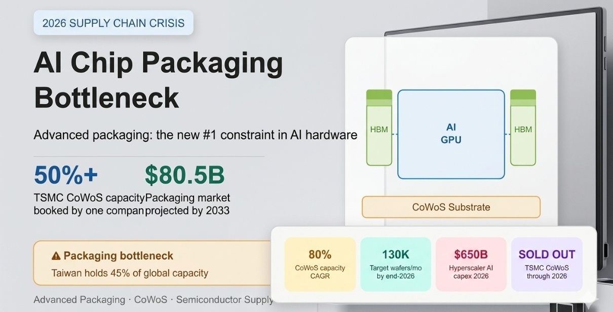
CoWoS (Chip-on-Wafer-on-Substrate) is the advanced packaging technology at the center of this story. Developed by TSMC, it allows logic chips and High Bandwidth Memory (HBM) to be co-integrated on a single silicon interposer, enabling the extreme memory bandwidth and compute density required by modern AI accelerators. Without CoWoS, an NVIDIA Blackwell GPU is just a collection of dies — not a product.
This deep dive covers what CoWoS is, why it is sold out, who wins and loses in this constrained environment, and what the next 18 months look like for AI infrastructure buyers, hyperscalers, and chip designers.
1. What Is CoWoS and Why Does Every AI Chip Need It?
Advanced chip packaging refers to the intricate process of combining multiple chiplets or dies — often from different nodes or suppliers — into a single high-performance package. These packages are critical to AI processors, cloud infrastructure chips, and autonomous systems. For more than five years, the move from monolithic chips to multi-die chiplet architectures has made advanced packaging indispensable.
CoWoS: The Architecture of AI Power
CoWoS integrates a logic die (such as a GPU) and stacks of High Bandwidth Memory (HBM) side by side on a silicon interposer. The interposer acts as a dense communication bridge, enabling memory bandwidth in the terabytes-per-second range — something that traditional package-on-board designs cannot approach. This bandwidth is what allows AI models with hundreds of billions of parameters to run efficiently.
Key facts about CoWoS in 2026:
- It is the packaging backbone for NVIDIA Blackwell, AMD MI350, and most leading AI accelerators
- Without CoWoS, fabricated AI dies cannot be turned into shippable products
- TSMC is the dominant supplier of CoWoS, with no peer at an equivalent scale
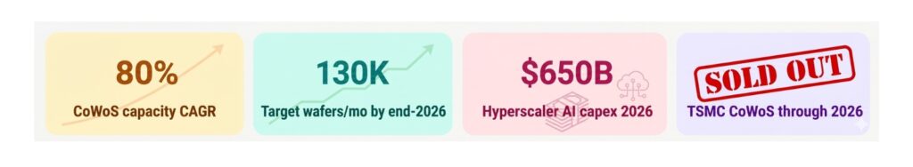
- Its CoWoS capacity is growing at an 80% compound annual growth rate — but demand still outpaces supply
📄 Further reading: Advanced Chip Packaging in Semiconductor Manufacturing (2025–2035) — Oplexa Market Research Report
2. The AI Chip Packaging Bottleneck in 2026: By the Numbers
The scale of the CoWoS shortage is significant enough to have direct revenue implications for some of the world’s largest technology companies. Here is what the data shows:
TSMC’s CoWoS Capacity Ramp
TSMC is executing one of the most aggressive capacity expansions in semiconductor history specifically to address this AI chip packaging bottleneck. The company is scaling CoWoS production from approximately 35,000 wafers per month in late 2024 to a projected 130,000 wafers per month by the end of 2026. That is nearly a 4x increase in under two years — and it is still not enough to fully satisfy demand.
TSMC’s CEO C.C. Wei has publicly acknowledged the severity: CoWoS capacity remains extremely tight and is sold out through 2026. The company has even begun outsourcing some packaging steps to specialized third-party firms such as ASE and Amkor to relieve pressure, with ASE projecting its own advanced packaging sales to double in 2026.
TSMC is also ramping new facilities:
- Two new packaging facilities in Taiwan (including the new Chiayi AP7 plant)
- Two packaging facilities in Arizona — though all U.S.-made chips still travel back to Taiwan for packaging today
- CoWoS expanding at 80% CAGR according to TSMC North America packaging solutions head Paul Rousseau
| Company / Entity | Role in CoWoS Ecosystem | 2026 Position |
|---|---|---|
| NVIDIA | Primary consumer of CoWoS | Reserved majority of TSMC capacity |
| AMD | Secondary consumer (MI350/MI400) | Competing for remaining allocation |
| TPU CoWoS user | Cut TPU 2026 production target ~25% | |
| TSMC | Sole volume CoWoS supplier | Expanding at 80% CAGR, still sold out |
| ASE / Amkor | Outsourced packaging partners | Beneficiary — sales doubling in 2026 |
| Intel | Alternative packaging (EMIB/Foveros) | Gaining as overflow option for others |
3. Who Wins and Who Loses in the Packaging Crunch?
Clear Winners
NVIDIA is the biggest beneficiary of the current allocation dynamic. By reserving the majority of TSMC’s most advanced CoWoS capacity, NVIDIA has effectively built a moat around its GPU supply chain. Competitors — including AMD, Google, and second-tier ASIC vendors — are left competing for the remainder or forced to explore alternatives.
ASE Group, the world’s largest outsourced semiconductor assembly and test company, is a secondary winner. With TSMC outsourcing CoWoS sub-steps to relieve its own backlog, ASE is seeing advanced packaging sales double. Amkor is in a similar position. Both companies are building new capacity aggressively.
Intel is emerging as an unexpected beneficiary. Its EMIB (Embedded Multi-die Interconnect Bridge) and Foveros 3D stacking technologies are not direct CoWoS replacements in terms of raw performance, but they are mature enough to handle AI inference ASICs and modular SoCs. With TSMC’s CoWoS booked out, chipmakers manufacturing logic at TSMC’s Arizona plant are now exploring Intel’s Rio Rancho, New Mexico facility for domestic packaging — a significant shift.
Clear Losers
Google is the most visible casualty of the CoWoS squeeze. Reports indicate the company has reduced its 2026 Tensor Processing Unit (TPU) production target from approximately 4 million to 3 million units — a roughly 25% cut — due to constrained access to CoWoS packaging capacity that NVIDIA locked up through priority allocations. This directly impacts Google Cloud’s AI compute roadmap.
Smaller ASIC startups and custom chip designers face the steepest challenges. Without the purchasing scale to secure long-term CoWoS allocation agreements, they risk multi-quarter delays in shipping their products — potentially allowing NVIDIA to consolidate its market position further during the delay.
📄 Related: Custom ASIC Market 2026: Why Hyperscalers Are Ditching NVIDIA — Oplexa Blog
4. HBM: The Other Half of the AI Packaging Equation
CoWoS does not exist in isolation. It is inseparable from High Bandwidth Memory (HBM), the other critical ingredient in AI accelerator packages. HBM sits next to the GPU die on the CoWoS interposer, and without it, the package is incomplete.
The HBM market is also in a supply crunch. SK Hynix, Micron, and Samsung — the three HBM suppliers — are all in a capacity-constrained environment. SK Hynix supplies the majority of HBM for NVIDIA’s Blackwell chips. Micron is ramping HBM4 for volume production in 2026. Samsung is repricing HBM contracts upward in the high-teens percentage range.
| Why HBM Matters for AI Chip Packaging
• HBM provides the extreme memory bandwidth AI models require (TB/s range) • Each AI accelerator package integrates multiple HBM stacks via CoWoS • HBM supply constraints compound CoWoS constraints — both must align for a chip to ship • HBM pricing is rising 15–20% in 2026 as suppliers reprice contracts • Micron’s HBM4 for volume production in 2026 adds new supply but competition remains intense |
📄 Related: Micron’s $25B Bet: Why AI Memory Is the Next Semiconductor Gold Rush — Oplexa Blog
5. The Broader AI Semiconductor Supply Picture in 2026
The CoWoS bottleneck is the most acute constraint, but it exists within a broader supply-demand imbalance across the AI chip supply chain. Global semiconductor sales reached $88.8 billion in February 2026 alone — a 61.8% year-on-year increase — as the industry tracks toward approximately $1 trillion in annual revenue for the first time.
TSMC, the foundational manufacturer for virtually all leading AI chips, posted a 58% profit increase in Q1 2026, beating estimates. The company forecasts full-year 2026 revenue growth exceeding 30% year-on-year. Its CFO noted that the AI segment is pulling all the weight even as traditional markets like smartphones and PCs remain mixed due to memory shortages.
TSMC’s fabs are sold out through 2028. The company is adding advanced chip fabrication in Tainan, Taiwan, planning a massive GigaFab expansion in Arizona, and launching 3nm production in Japan in 2028. The four largest hyperscalers — Microsoft, Google, Amazon, and Meta — collectively committed $650 billion in AI infrastructure capital expenditure in 2026, a 71% year-on-year increase, ensuring demand will not slow.
Geopolitical Dimension
The packaging bottleneck also has a geopolitical dimension that is not widely discussed. TSMC currently sends 100% of its chips to Taiwan for packaging — including those manufactured at its advanced Phoenix, Arizona facility. This means U.S.-made AI chips are still dependent on Taiwanese packaging infrastructure. The U.S. government’s push for domestic AI supply chains runs directly into this reality. Until domestic packaging capacity is operational at scale (TSMC’s Arizona packaging facilities are still years from full ramp), the bottleneck will remain a point of national technology policy concern.
📄 Deep dive: TSMC AI Investment: The $7 Trillion Bet Nobody Talks About — Oplexa Blog
6. What Comes Next: 2026–2028 Packaging Technology Roadmap
The CoWoS constraint is driving investment and innovation in alternative packaging approaches that could reshape competitive dynamics by 2027–2028:
Panel-Level Packaging
Moving from round 12-inch wafers to rectangular panels dramatically increases usable area — from approximately 57% to over 80% efficiency. As AI chips grow in die size (some exceeding the reticle limit), panel-level packaging becomes economically essential. This technology is expected to enter production at scale by 2027.
Glass Substrates
Glass offers superior flatness and thermal stability compared to organic substrates used today — critical properties for the sub-2nm circuitry of future AI chips. Industry analysts predict that the first commercial applications of glass-based advanced packaging will appear by late 2027, extending CoWoS-class performance gains into the next process generation.
Co-Packaged Optics (CPO)
As data volumes inside AI chips continue to grow, copper interconnects are hitting bandwidth limits. Co-packaged optics integrates optical communication directly into the chip package, dramatically increasing bandwidth while reducing power consumption. First commercial AI chips featuring CPO are expected in high-end data centers within 18 to 24 months.
Intel EMIB and Foveros as Near-Term Alternatives
For the AI inference market — where absolute peak performance requirements are somewhat lower than training — Intel’s EMIB and Foveros technologies offer a viable near-term alternative to CoWoS. They are mature, commercially available, and can be performed at Intel’s domestic U.S. facilities, making them attractive to chipmakers facing TSMC CoWoS allocation constraints and seeking domestic packaging pathways.
📄 Related: Intel Terafab Project: The $25B Gamble to Rewire AI Infrastructure — Oplexa Blog
7. What This Means for Enterprise Buyers, CTOs, and Investors
| Stakeholder | Key Risk | Strategic Action |
|---|---|---|
| Enterprise Buyers | Delayed AI hardware delivery, rising prices | Lock in multi-year GPU/accelerator contracts now |
| Cloud Architects | Limited instance availability on AWS/Azure/GCP | Plan for CoWoS-constrained supply through 2026 |
| Chip Investors | CoWoS allocation = revenue ceiling for some cos. | Track ASE, Amkor, Micron as packaging beneficiaries |
| AI Startups | Custom ASIC delays up to several quarters | Consider inference-optimized off-the-shelf GPUs as bridge |
| Data Center Planners | Power + packaging constraints co-exist | Factor 20%+ HBM price increases into 2026 capex models |
Conclusion
Advanced chip packaging — and CoWoS in particular — has transformed from a back-end afterthought into the primary determinant of who can ship AI hardware at scale in 2026. The companies that secured early CoWoS allocation (led by NVIDIA) have a structural advantage that is difficult to overcome on short timelines. Those that did not (including Google for its TPU program) are absorbing real production shortfalls.
For enterprise technology leaders, the AI chip packaging bottleneck in 2026 is not an abstract supply chain talking point. It is a concrete constraint on when AI infrastructure gets built, at what cost, and from whom. Tracking packaging capacity as closely as silicon fabrication is now essential operational intelligence.
The resolution — through TSMC’s CoWoS expansion, panel-level packaging, glass substrates, and domestic U.S. packaging capacity — is underway. But the window of constraint is measured in years, not quarters. Plan accordingly.
Frequently Asked Questions
Q: What is the CoWoS AI chip packaging bottleneck?
A: CoWoS (Chip-on-Wafer-on-Substrate) is TSMC’s advanced packaging technology that integrates AI processor dies with High Bandwidth Memory on a silicon interposer. In 2026, global CoWoS capacity is sold out because demand from AI hyperscalers — led by NVIDIA — far exceeds TSMC’s ability to produce it. Without CoWoS, fabricated AI chips cannot be turned into functional products.
Q: Why is NVIDIA able to secure CoWoS capacity while others cannot?
A: NVIDIA reserved the majority of TSMC’s most advanced CoWoS capacity through long-term allocation agreements, prioritizing its position as TSMC’s largest customer. This gives NVIDIA a structural supply chain moat. Other chip designers — including Google for its TPUs and AMD for its MI-series — are competing for the remaining allocation.
Q: How long will the AI chip packaging bottleneck last?
A: TSMC is scaling CoWoS capacity from 35,000 wafers/month (late 2024) to 130,000 wafers/month by end of 2026. However, with hyperscaler capex commitments of $650 billion for AI infrastructure in 2026 alone, the constraint environment is expected to persist through 2027 in varying degrees, particularly for second-tier chipmakers and custom ASIC vendors.
Q: What alternatives exist to TSMC CoWoS for AI chip packaging?
A: Intel’s EMIB and Foveros technologies are the primary near-term alternatives, particularly for AI inference ASICs. ASE and Amkor are also expanding outsourced packaging capacity as TSMC offloads some CoWoS sub-steps. Longer term, panel-level packaging and glass substrates will offer new options, but commercial deployments are not expected until 2027–2028.
Q: How does the CoWoS bottleneck affect AI cloud services in 2026?
A: Constrained CoWoS supply limits how many AI accelerators cloud providers like AWS, Google Cloud, and Microsoft Azure can deploy. Google has already cut its 2026 TPU production target by approximately 25% due to CoWoS access constraints. This translates to tighter availability and potential price increases for AI compute instances on major cloud platforms.
Oplexa is an independent AI and semiconductor intelligence platform covering chip architecture, supply chain dynamics, and AI infrastructure strategy. Our analysis is designed for technology professionals, enterprise decision-makers, and investors navigating the fast-moving landscape of AI hardware.
Visit: https://oplexa.com | For AI & semiconductor deep dives
1 Comment