By Carter James | Oplexa Insights
Mar 2026 | 18 Min Read
Everyone is watching NVIDIA. Everyone is debating Broadcom. Everyone is tracking custom ASICs. But almost nobody is talking about the one company that sits beneath all of them — the company that literally manufactures the chips that power the entire AI era.
Taiwan Semiconductor Manufacturing Company — better known as TSMC — is not a chip designer. It does not compete with NVIDIA, Broadcom, or Google’s TPU team. It is the foundry that makes all of its chips. And that positioning — supplier to every major player simultaneously, regardless of who wins the AI arms race — makes the TSMC AI investment thesis one of the most compelling in the semiconductor industry today.
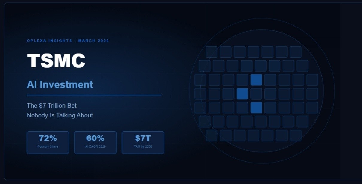
McKinsey estimates $7 trillion will be spent building AI data centers by 2030. TSMC will manufacture the chips that power a significant share of that infrastructure. With 72% of the global foundry market, a 60% CAGR forecast for AI chip revenue through 2029, and $165 billion committed to U.S. expansion, TSMC is positioned to capture AI spending regardless of which chip architecture ultimately wins.
Why TSMC Is the ‘Pick-and-Shovel’ Play of the AI Era
The gold rush analogy is overused in investing — but for TSMC, it is genuinely apt. During the California Gold Rush, the companies that reliably made money were not the miners gambling on finding gold. They were the suppliers of picks, shovels, and denim pants — the infrastructure providers whose revenue was guaranteed regardless of which miner struck it rich.
TSMC occupies exactly this position in the AI chip market. Whether NVIDIA’s Vera Rubin architecture dominates AI training, or Google’s TPU captures inference, or Broadcom’s custom ASICs win hyperscaler deployments — every one of these chips is manufactured at TSMC. The foundry does not care who wins the design war. It gets paid on every chip that ships.
| 💡 The TSMC Advantage: Indifferent to the Chip War Outcome
NVIDIA, AMD, Broadcom, Google, Meta, Amazon, Apple, and Intel all use TSMC as their primary advanced-node manufacturer. When investors debate which chip company will win in AI, they are debating which product TSMC will manufacture the most of. TSMC wins either way. |
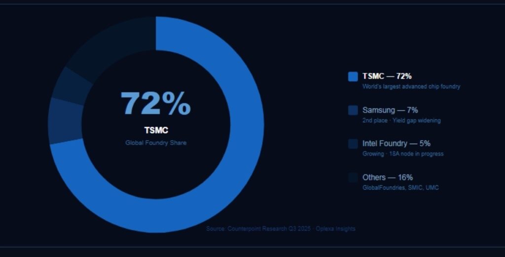
This structural positioning has produced extraordinary financial results. In Q3 2025, TSMC’s foundry revenue grew more than 40% year over year — significantly outpacing the broader semiconductor market’s 17% growth. Advanced technologies below 7nm now account for nearly 75% of TSMC’s wafer revenue, underscoring that the highest-margin, AI-critical chips are its fastest-growing business segment.
🔗 Read also: Custom ASIC Market 2026: Why Hyperscalers Are Ditching NVIDIA
The $165 Billion U.S. Expansion — Building the Future of AI Infrastructure
The most significant strategic development in the global semiconductor supply chain in 2026 is TSMC’s $165 billion U.S. manufacturing expansion — officially the largest single foreign direct investment in American history. This investment is not driven solely by patriotism or political pressure. It is driven by the structural reality that TSMC’s customers—primarily U.S. technology companies—want their chip supply chains closer to home.
TSMC U.S. Arizona Expansion — Facility Breakdown
| Facility | Node | Timeline | Purpose |
| Fab 1 (Phoenix) | 4nm | In production 2024 | iPhone + AI chips |
| Fab 2 (Phoenix) | 3nm / 2nm | 2026–2027 | NVIDIA / AMD AI chips |
| Fab 3 (Phoenix) | A16 1.6nm | 2028+ | Next-gen AI frontier |
| Packaging x2 | CoWoS Advanced | 2025–2027 | HBM integration |
| R&D Center | Multiple nodes | Ongoing | Next-gen process dev. |
| Total Investment | $165 Billion — Largest single FDI in U.S. history · 40,000+ construction jobs |
The Arizona expansion is strategically significant beyond its scale. It directly addresses the primary risk that institutional investors cite about TSMC: geographic concentration. With most of TSMC’s current capacity located in Taiwan, within 100 miles of the Chinese coastline, any geopolitical escalation would create a supply shock that would affect every major technology company simultaneously. The U.S. expansion reduces this concentration risk while also qualifying TSMC for CHIPS and Science Act funding.
| 📊 Oplexa Research Report
Global Semiconductor Supply Chain Risk & Forecast 2025–2035 TSMC geographic risk, fab expansion analysis, geopolitical semiconductor exposure & supply chain investment implications |
$299 |
TSMC’s Technology Moat — Why Nobody Can Catch Up
Understanding the TSMC AI investment thesis requires understanding why no competitor can replicate TSMC’s capabilities. The answer lies in three interlocking advantages that have taken decades to build and would take a decade more to replicate.
1. Advanced Node Leadership — 3nm and 2nm
TSMC’s 3-nanometer process node — currently manufacturing NVIDIA’s Vera Rubin GPU and Apple’s M-series chips — is the most advanced semiconductor process in commercial volume production. The company’s N2 node (2nm), launching in volume production in 2025, further extends this lead. For context, Samsung’s comparable process node yields approximately 20-30% lower than TSMC’s — meaning Samsung must manufacture significantly more chips to deliver the same number of functional units, at dramatically higher cost.
The gap is not closing. TSMC’s R&D spending — $6.9 billion in 2025 — exceeds Samsung’s entire foundry revenue. Every generation of process technology TSMC advances widens the moat, because catching up requires mastering the current generation before the next one renders it obsolete.
2. CoWoS Advanced Packaging — The HBM4 Connection
Chip-on-Wafer-on-Substrate (CoWoS) is TSMC’s proprietary advanced packaging technology that enables multiple chips—including HBM4 memory stacks—to be integrated on a single substrate with extremely short interconnect distances. Every NVIDIA GPU, every Google TPU, and every custom ASIC using HBM4 memory requires CoWoS packaging. TSMC is the dominant provider of this technology.
The significance of CoWoS cannot be overstated. A Vera Rubin GPU is not simply a piece of silicon — it is a complex assembly of compute die, HBM4 memory stacks, and networking components, all integrated via CoWoS. TSMC’s packaging capability is as essential to AI chip performance as its transistor density. This creates a second layer of customer dependency that reinforces the primary manufacturing relationship.
3. Customer Ecosystem Lock-In
TSMC’s customers — NVIDIA, Apple, Broadcom, AMD, Google, Amazon, Microsoft, and Intel — have each invested years and billions of dollars optimising their chip designs for TSMC’s specific process nodes. Switching foundries is not simply a matter of moving production to another facility. It requires redesigning the chip from scratch to match the electrical characteristics, layout rules, and design library of a different process. The switching cost for a major chip design is $500 million to $1 billion in engineering time and tape-out costs, and a two- to three-year delay.
| 📊
TSMC Technology Stack — 5nm → 3nm → 2nm → A16 Advanced nodes · CoWoS packaging · High-NA EUV · Silicon photonics (A16) |
The $720 Billion Hyperscaler Tailwind
The most powerful driver of the TSMC AI investment thesis is not TSMC itself — it is the capital expenditure plans of its largest customers. The five major hyperscalers have collectively guided for $720 billion in AI infrastructure capital expenditure in 2026 alone.
Hyperscaler AI Capital Expenditure — 2026 Guidance
| Hyperscaler | 2026 CapEx Guidance | YoY Growth | TSMC-manufactured chips |
| Microsoft Azure | $80B+ | +40% | Vera Rubin + Maia ASIC |
| Amazon AWS | $100B+ | +35% | Trainium 3 + Inferentia |
| Alphabet (Google) | $75B+ | +42% | TPU v8 Trillium |
| Meta | $65B+ | +38% | MTIA 400 + GPUs |
| Oracle / Others | $400B+ | +45% | NVIDIA GPU clusters |
| Total 2026 | ~$720 Billion in AI CapEx · TSMC manufactures chips for all of it |
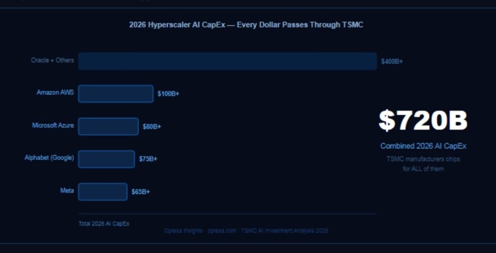
The critical insight for investors is that TSMC captures a percentage of every dollar in this $720 billion. Not all of it — hyperscalers also spend on data center construction, power infrastructure, networking equipment, and software. But the chip component of AI infrastructure spending flows directly through TSMC’s advanced node fabs. As the only supplier capable of manufacturing the most advanced AI chips at volume, TSMC functions as a toll booth on the AI capital expenditure highway.
| 📊 Oplexa Research Report
AI Infrastructure Strategy 2026–2035: Capital & Compute Hyperscaler CapEx analysis, TSMC dependency mapping & AI infrastructure investment thesis |
$999 |
TSMC’s Financial Performance — The Numbers Behind the Thesis
TSMC Financial Snapshot — Key Metrics 2025–2026
| Metric | 2025 Actual | 2026 Analyst Estimate |
| Revenue | $122B (+31% YoY) | $158B (+30% forecast) |
| HPC Revenue Share | 58% of total revenue | 65%+ (AI-driven) |
| HPC YoY Growth | +48% year over year | 50%+ expected |
| Gross Margin | ~57% | 58-60% (pricing power) |
| Foundry Market Share | 72% (Q3 2025) | 73-75% (expanding) |
| CapEx Investment | $50B (2025) | $52-56B (2026 guidance) |
| Forward P/E | ~30x | 23.6x (current) |
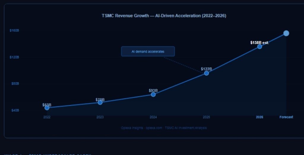
The valuation metrics tell a compelling story. TSMC’s forward P/E ratio of 23.6x sits below the broader semiconductor industry average of 44.5x — despite the company growing revenue faster than almost any comparable business at its scale. For investors who prefer growth at a reasonable price, TSMC’s combination of 30%+ revenue growth and sub-sector-average valuation is unusual in the current market environment.
| 📊
TSMC Revenue Growth 2022–2026 — AI-Driven Acceleration $65B (2022) → $70B (2023) → $93B (2024) → $122B (2025) → $158B est. (2026) |
Key Risks to the TSMC AI Investment Thesis
| ⚠️ Geopolitical Risk — Taiwan Strait
TSMC’s primary manufacturing concentration in Taiwan remains the most cited investor concern. While TSMC is actively expanding globally in Arizona, Japan, and Germany, the majority of its 3nm and 2nm capacity will remain in Taiwan for the foreseeable future. Any military action in the Taiwan Strait would trigger a global chip supply shock that would affect every technology company worldwide. TSMC’s stock would be severely impacted even before any physical disruption occurred. |
| ⚠️ Concentration Risk — NVIDIA Dependency
NVIDIA has grown to become TSMC’s largest single customer. As NVIDIA’s revenue represents an increasingly large share of TSMC’s advanced node utilisation, any slowdown in NVIDIA GPU demand — whether from macroeconomic factors, competitive displacement, or hyperscaler spending pauses — would disproportionately impact TSMC’s advanced node revenue. |
| ⚠️ U.S. Overseas Fab Cost Pressure
TSMC’s Arizona fabs operate at significantly higher costs than its Taiwan facilities — reflecting higher U.S. labor costs, regulatory requirements, and supply chain complexity. As overseas capacity scales, TSMC’s gross margins could be compressed unless it successfully negotiates higher premiums from customers who require U.S.-manufactured chips. This margin pressure could emerge as early as 2027. |
| ⚠️ Samsung and Intel Foundry Catch-Up Risk
Samsung’s 2nm process and Intel’s 18A node are both targeting production in 2025-2026. While neither has historically matched TSMC’s yield rates, sustained investment could narrow the gap over a 3-5-year horizon. If Samsung or Intel Foundry successfully captures meaningful advanced-node market share, TSMC’s pricing power and margin structure could erode. |
| 📊 Oplexa Research Report
Semiconductor Fab Design & Construction Market Trends 2025–2035 Global fab expansion analysis, cost structures, yield comparison & competitive foundry landscape |
$999 |
5 Key Takeaways for Investors
1 | TSMC AI investment thesis is architecture-agnostic. Whether NVIDIA, custom ASICs, or a new architecture wins AI — TSMC manufactures the chips. The investor does not need to predict which chip design wins. They only need to believe that AI infrastructure spending will continue growing.
2 | $720 billion in hyperscaler CapEx is a direct TSMC tailwind. Every dollar hyperscalers spend on AI chips flows through TSMC’s advanced fabs. With $720 billion in committed 2026 AI CapEx and a 30%+ revenue growth forecast, TSMC’s near-term revenue visibility is among the strongest in the semiconductor industry.
3 | The 60% AI chip CAGR forecast is management guidance, not an analyst projection. TSMC’s own management forecast of 60% CAGR for AI chip revenue through 2029 is one of the most aggressive growth projections ever made by a company of its scale. Even if actual growth comes in at 40% — two-thirds of the forecast — TSMC’s revenue trajectory would be transformational.
4 | Valuation is arguably attractive relative to growth. TSMC’s forward P/E of 23.6x sits below the semiconductor industry average of 44.5x, despite growing revenue at 30%+ annually. The PEG ratio of approximately 1.1 suggests the market is pricing in execution risk but not a premium for TSMC’s structural advantages.
5 | The $165 billion U.S. expansion reduces the single biggest investor concern. TSMC’s Arizona expansion directly addresses the geopolitical risk that has historically suppressed its valuation. As U.S. capacity scales through 2027-2028, the geographic concentration discount that the market applies to TSMC should gradually compress — a potential re-rating catalyst independent of revenue growth.
Conclusion
The TSMC AI investment thesis is deceptively simple: when the entire world is building AI infrastructure, the company that manufactures the chips for all of it is positioned to capture an extraordinary share of the resulting value. The $7 trillion data center spending wave projected by McKinsey through 2030 will require trillions of advanced semiconductor chips. TSMC will manufacture the majority of them.
This is not a bet on a single chip architecture, a single hyperscaler’s AI strategy, or a single model generation. It is a bet on the continued growth of AI infrastructure spending and TSMC’s structural position as the only company capable of manufacturing the most advanced chips at commercial scale. That position — built over three decades and protected by capital-intensive moats that competitors cannot close in a decade — is the foundation of one of the most durable investment theses in the semiconductor industry.
| 🔑 The Core TSMC Investment Thesis
TSMC is not betting on who wins the AI chip war. It is the factory that manufactures the weapons for all sides. With 72% foundry market share, a 60% AI chip CAGR forecast, $165B in U.S. expansion, and a valuation below the sector average — the TSMC AI investment thesis rests on one simple question: will AI infrastructure spending continue growing? Every major data point in 2026 says yes. |
🔗 Read also: Micron’s $25B Bet: Why AI Memory Is the Next Semiconductor Gold Rush
🔗 Read also: Custom ASIC Market 2026: Why Hyperscalers Are Ditching NVIDIA
🔗 Read also: GTC 2026 Wrap-Up: 10 Biggest NVIDIA Announcements
Frequently Asked Questions
What makes TSMC different from other semiconductor companies?
TSMC is a pure-play foundry — it only manufactures chips, never designs them. This means it never competes with its customers, making it the trusted manufacturing partner for companies that do compete with each other, including NVIDIA, AMD, Apple, and Broadcom. Its 72% global foundry market share, 3nm process leadership, and proprietary CoWoS advanced packaging create a combination of scale and capability advantages that competitors have been unable to replicate despite decades of investment.
Why does TSMC benefit from the AI investment boom?
Every major AI chip — NVIDIA’s Vera Rubin GPU, Google’s TPU, Apple’s M-series, Broadcom’s custom ASICs, and Amazon’s Trainium — is manufactured at TSMC. As hyperscalers commit $720 billion in AI capital expenditure in 2026 alone, a significant portion of that spending requires TSMC’s advanced fabrication capabilities. TSMC’s management has forecast that AI chip revenue will grow at a 60% CAGR through 2029, driven by this structural demand.
What is the biggest risk to TSMC’s AI investment thesis?
Geopolitical risk — specifically the possibility of military conflict in the Taiwan Strait — is the most commonly cited concern. The majority of TSMC’s advanced node manufacturing capacity is currently located in Taiwan, close to the Chinese coastline. Any disruption to Taiwanese sovereignty would cause a global chip supply shock. TSMC is actively mitigating this risk through $165 billion in U.S. expansion and facilities in Japan and Germany, but geographic diversification will take years to meaningfully reduce the concentration risk.
How does TSMC’s $165 billion U.S. expansion affect its investment thesis?
The Arizona expansion addresses the primary valuation suppressor for TSMC — its geographic concentration in Taiwan. As U.S. fabs ramp production through 2026-2028, the geopolitical risk discount that markets apply to TSMC should gradually compress. Additionally, U.S.-manufactured chips command price premiums from customers who require domestic supply chains, which could support margin expansion even as facility costs are higher than those of Taiwan-based manufacturing.
How does TSMC connect to other AI infrastructure companies like NVIDIA and Broadcom?
TSMC is the manufacturing backbone for the entire AI chip ecosystem. NVIDIA’s Vera Rubin GPU is manufactured on TSMC’s 3nm process. Broadcom’s custom ASIC designs — powering Google’s TPU, Microsoft’s Maia, and Meta’s MTIA — are also fabricated at TSMC. Micron’s HBM4 memory, which integrates with TSMC-made compute chips via TSMC’s CoWoS packaging technology, completes the picture. Understanding TSMC is essential to understanding the full AI infrastructure supply chain.
1 Comment