By Mitthan Meena | Oplexa Insights
April 2026 | 09 Min Read
Introduction: A New Era of Industrial Intelligence
On April 7, 2026, the semiconductor world witnessed a tectonic shift. Intel CEO Lip-Bu Tan and Elon Musk officially announced that Intel would serve as the manufacturing backbone for the Intel Terafab Project. This is not merely a factory; it is a $25 billion vertically integrated mega-complex in Austin, Texas, designed to produce 1 terawatt of AI compute annually.
For years, the AI chip market has been bottlenecked by a single point of failure: geographic concentration in East Asia. The Intel Terafab Project changes that narrative. By bringing design, fabrication, and advanced packaging under one roof on the North Campus of Giga Texas, this venture represents the most audacious attempt at semiconductor self-sufficiency in American history.
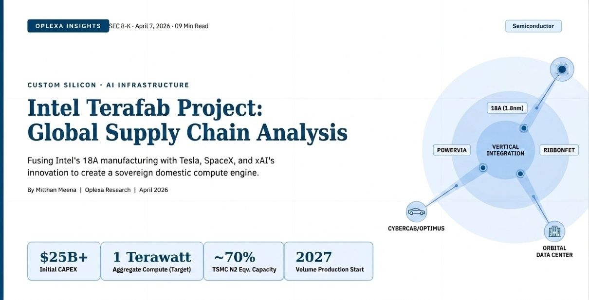
Understanding the Architecture: What is the Intel Terafab Project?
The Intel Terafab Project is structured to solve the “shipping bottleneck.” In traditional manufacturing, a chip is designed in the US, fabricated in Taiwan, and packaged in Malaysia. The Intel Terafab Project eliminates this by consolidating the entire lifecycle within a single facility.
The Two Pillars of Terafab
-
Terrestrial AI Infrastructure: This wing focuses on the Tesla AI5 chip, a 5th-generation inference engine designed for the Cybercab and Optimus robots. The goal is to produce 100,000 wafer starts per month by early 2027.
-
Orbital AI Infrastructure: This is where the project enters “moonshot” territory. SpaceX recently filed with the FCC for a million-satellite constellation equipped with AI accelerators. The Intel Terafab Project will produce radiation-hardened variants of these chips, enabling distributed Orbital Data Centers that harvest solar power directly in space.
Why Intel? The Foundry Turnaround of the Decade
Intel’s participation in the Intel Terafab Project is the ultimate validation of its IDM 2.0 strategy. But why did Musk choose Intel over TSMC or Samsung?
1. The 18A (1.8nm) Logic Leadership
Intel’s 18A process node is the star of the Intel Terafab Project. With PowerVia (backside power delivery) and RibbonFET architecture, 18A offers a significant performance-per-watt advantage over current 3nm technologies. For robots like Optimus, battery life and thermal efficiency are everything—making 18A the only viable domestic choice.
2. Solving the 18A Yield Challenge
Critics have pointed to low yields in the past, but by April 2026, Intel reported that 18A yields have stabilized at 62%, sufficient for the initial ramp of the Intel Terafab Project. The partnership with Tesla provides the high-volume “learning cycles” Intel needs to push yields toward the 80% industry gold standard.
📊 Related Report: Global Semiconductor Supply Chain Risk & Forecast (2025–2035) — A detailed look at how Intel 18A compares to TSMC N2 and Samsung SF2 nodes.
Impact on the Global Semiconductor Supply Chain
The Intel Terafab Project is a direct response to the fragile state of the global semiconductor supply chain.
The “TSMC Dependency” Exit Strategy
Currently, 90% of advanced AI chips come from a single island. The Intel Terafab Project creates a “Western Fortress” for silicon. By 2028, if the Austin facility hits its target of 1 million wafer starts per month, it will represent nearly 70% of TSMC’s current global output from a single location.
Geopolitical Shielding: The US-China Chip War
As export restrictions tighten, the Intel Terafab Project ensures that the US has a closed-loop ecosystem for its most sensitive AI technologies. This is analyzed deeply in our report on the US-China Chip War 2026, where domestic “sovereign foundries” are identified as the only long-term defense against supply chain weaponization.
The Rise of Custom ASICs: Beyond the GPU
The Intel Terafab Project signals the end of the “GPU-only” era. Musk has been vocal about the inefficiency of general-purpose hardware for specific tasks.
Vertical Integration and Performance
By building Custom ASICs at the Intel Terafab Project, Tesla and SpaceX can strip away the overhead of general-purpose silicon. This trend is mirrored by other hyperscalers, as seen in the Broadcom Google TPU Deal 2026. When you control the fab (Intel) and the design (Tesla), you can optimize for milliwatts of power—a necessity for millions of autonomous devices.
Re-Evaluating the Semiconductor Industry Market Size
Current projections for the semiconductor industry market size often focus on terrestrial data centers and consumer electronics. However, the Intel Terafab Project introduces a new variable: Space-as-a-Service.
-
Market Expansion: Global revenue is expected to hit $1.3 trillion in 2026.
The SpaceX Factor: If even 10% of SpaceX’s orbital compute goals are met, it creates a $100B+ sub-market for specialized, high-reliability chips that didn’t exist two years ago.
📊 Related Data: GAA Transition & Impact on Semiconductor Capital Equipment (2025-2035) — Understanding the machinery required to build the Intel Terafab Project.
Risks: Execution, Capital, and Physics
No project of this scale is without risk. For the Intel Terafab Project, the challenges are three-fold:
-
Thermal Management in Orbit: Cooling high-performance chips in a vacuum requires massive radiative panels, a challenge SpaceX is still iterating on with Starlink V3.
-
Capital Burn: Tesla’s negative free cash flow in Q1 2026 puts pressure on the Intel Terafab Project’s $25B budget.
-
ASML Bottleneck: To hit 1 million wafers, the project needs a significant portion of ASML’s global High-NA EUV output, which is currently oversubscribed.
5 Strategic Takeaways for 2026
-
Sovereign Compute: The Intel Terafab Project is the first true “Sovereign AI” facility—domestic, vertically integrated, and immune to foreign supply shocks.
-
The Death of “Fabless” Identity: Top-tier companies are becoming “Fab-Adjacent,” working directly in the facility with the foundry.
-
18A is the New Gold Standard: If Intel executes the Intel Terafab Project, 18A becomes the default node for the next generation of AI robotics.
-
Orbital Intelligence is Real: Space is the new frontier for data centers, solving the terrestrial power and cooling crisis.
-
Diversify Hardware Portfolios: The AI chip market is diversifying. Leaders must look beyond NVIDIA toward custom silicon solutions born out of facilities like Terafab.
Conclusion
The Intel Terafab Project is not just another manufacturing headline; it is a structural realignment of the global technology balance of power. By fusing Intel’s deep-rooted manufacturing heritage with the aggressive, “fail-fast” innovation of the Musk ecosystem—Tesla, SpaceX, and xAI—this venture creates a revolutionary blueprint for the future of the semiconductor supply chain.
For decades, the industry operated under the “Fabless” model, where design happened in the West and fabrication happened in the East. The Intel Terafab Project effectively ends that era. It signals a return to vertical integration at a scale never seen before—where the same campus that designs the neural networks also prints the silicon and packages the hardware.
As we look toward 2027 and beyond, the success of this project will be the litmus test for America’s semiconductor sovereignty. If Intel can successfully execute the 18A ramp within the Austin complex, the reliance on single-geography foundries will diminish, giving rise to a more resilient, distributed, and domestic AI Infrastructure.
The massive Capital Expenditure being poured into Austin today is the down payment on the intelligence of tomorrow. We are moving past the age of simple “chip design.” With the Intel Terafab Project, we are witnessing the birth of a sovereign compute engine—one that will power everything from humanoid robots on factory floors to autonomous satellites in low Earth orbit. We are no longer just dreaming of the future in America; we are building it, atom by atom, in Austin.
Further Reading from Oplexa:
Frequently Asked Questions (FAQs)
Q: Why is it called the “Terafab”?
A: The “Tera” refers to the project’s goal of producing one terawatt of aggregate AI compute capacity annually through its chip output.
Q: When will the first chips from the Intel Terafab Project be ready?
A: Pilot production of the AI5 chip is expected in late 2026, with volume production ramping up throughout 2027.
Q: Is the Intel Terafab Project open to other customers?
A: Currently, it is a dedicated venture for the Musk ecosystem (Tesla, SpaceX, xAI), though Intel may use the “refactored” technology developed here for other foundry customers in the future.