By Carter James | Oplexa Insights
May 2026 | 18 Min Read
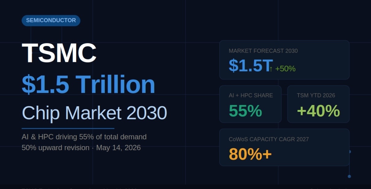
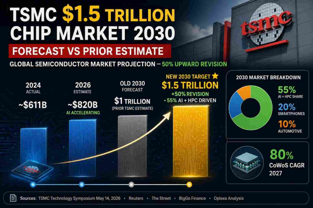
On May 14, 2026, TSMC raised its long-term semiconductor market forecast by 50% in a single announcement. The world’s largest contract chipmaker now projects the TSMC $1.5 trillion chip market by 2030 — up from its earlier estimate of $1 trillion — with AI and high-performance computing driving 55% of total demand. TSM stock is already up 40% in 2026 alone, and the TSMC $1.5 trillion chip market 2030 forecast signals there is more runway ahead.
For investors, enterprise architects, and AI infrastructure teams, the TSMC $1.5 trillion chip market 2030 announcement is the clearest confirmation yet that the AI hardware buildout is structural, not cyclical. When the company that manufactures chips for NVIDIA, Apple, AMD, Broadcom, Google, and Amazon raises its decade-end market forecast by $500 billion, it is not guessing. It is reflecting committed customer demand already visible in its order books and CoWoS packaging queues.
This is Oplexa’s complete breakdown of the TSMC $1.5 trillion chip market 2030 forecast — what drove the revision, the full new node roadmap, the A16 delay impact, CoWoS capacity expansion numbers, and exactly which companies benefit most from this structural shift in semiconductor demand.
TSMC $1.5 Trillion Chip Market 2030 — Why the 50% Revision Is Credible
The TSMC $1.5 trillion chip market 2030 forecast is not a marketing number. TSMC is the most capacity-constrained company in the global technology supply chain — it manufactures chips for every major AI accelerator company on earth. When TSMC raises its long-term forecast by $500 billion, it is reflecting demand already committed in customer purchase orders, not speculative projections.
Three structural forces drove the TSMC $1.5 trillion chip market 2030 revision:
1. AI Chips Generate 4–6x More Revenue Per Wafer Than Smartphones
A smartphone SoC and an AI GPU both use TSMC’s leading-edge process nodes. But they create fundamentally different revenue profiles. A single NVIDIA Blackwell B200 GPU die costs $5,700–$7,300 to manufacture and uses 4–6x more wafer area than a smartphone processor. AI chips also require CoWoS advanced packaging — adding $2,000–$5,000 in incremental revenue per chip above the wafer cost. Every AI chip TSMC manufactures generates significantly more revenue than any smartphone chip it displaces. The TSMC $1.5 trillion chip market 2030 reflects this revenue intensity shift — not just unit volume growth in the traditional sense.
2. $700B in Hyperscaler Capex Is Committed and Visible in TSMC’s Order Book
Microsoft, Google, Amazon, and Meta have collectively committed over $700 billion in 2026 AI infrastructure capital expenditure. The majority flows directly or indirectly to TSMC — through NVIDIA GPU procurement on TSMC N3, Broadcom-designed TPU and MTIA chips for Google and Meta, and Amazon’s Trainium 3 on TSMC 3nm. CEO C.C. Wei has described AI demand as structural rather than cyclical. The TSMC $1.5 trillion chip market 2030 is the extrapolation of demand TSMC can already see in its leading-edge wafer order book today.
3. CoWoS Capacity Growing at 80% CAGR — TSMC Only Builds What Customers Have Committed
TSMC’s CoWoS advanced packaging capacity is growing at over 80% CAGR through 2027. TSMC does not speculatively build advanced packaging capacity — it builds against committed customer purchase orders. The TSMC $1.5 trillion chip market 2030 capacity buildout, including nine fab phases in 2026 alone, represents one of the largest manufacturing infrastructure investments in corporate history. Nine phases means nine factories being built simultaneously — only rational if the underlying demand is real and contracted.
“AI is expected to replace smartphones as the semiconductor industry’s primary growth driver over the coming decade.” — TSMC Technology Symposium, Hsinchu, May 14, 2026
📊 Oplexa Report: AI Chip Market Analysis & Forecast 2025–2035 — $1,499 — Full TSMC revenue model by node, AI chip demand scenarios, CoWoS capacity analysis, and 10-year investment thesis for the $1.5 trillion chip market.
TSMC Roadmap 2026–2029 — Every Node That Matters for AI Chips
The TSMC $1.5 trillion chip market 2030 forecast lands alongside the most detailed public technology roadmap TSMC has ever published. Every major AI accelerator shipping in 2026–2029 is tied to a specific TSMC process node — understanding the timeline is essential for evaluating AI chip stocks and enterprise GPU procurement decisions.
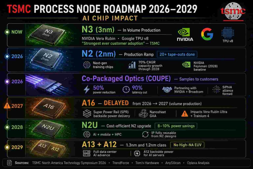
TSMC A16 Delay — Direct Impact on NVIDIA Vera Rubin Ultra and Trainium 4
The most operationally significant update in the TSMC $1.5 trillion chip market 2030 roadmap announcement is the A16 volume production delay from 2026 to 2027. For AI chip investors and enterprise procurement teams, this has concrete near-term implications.
What A16 Is and Why It Matters for AI
A16 is TSMC’s first process node to feature Super Power Rail (SPR) — a backside power delivery network that moves power routing to the back of the wafer. This frees the front side for signal routing only, dramatically reducing voltage loss in the dense, power-hungry AI accelerators that drive the TSMC $1.5 trillion chip market 2030 growth trajectory. For AI chips specifically, backside power delivery is not a convenience — it is becoming a first-order design constraint as power consumption per rack continues rising.
A16 Delay — What It Impacts
The A16 delay directly affects NVIDIA Vera Rubin Ultra (H2 2027) and Amazon Trainium 4 (targeting late 2026/early 2027). Both were designed around A16-class improvements. They will either push to late 2027 or launch on N2-class processes with performance trade-offs. Importantly, the TSMC $1.5 trillion chip market 2030 does not hinge on A16 in 2026 — everything shipping this year uses N3 and N2, which are already in volume production. The delay is a 2027 product cycle issue, not a 2026 supply constraint.
What the Delay Does Not Change
The A16 delay does not affect the TSMC $1.5 trillion chip market 2030 structural thesis. N2 capacity is growing at 70% CAGR through 2028. CoWoS yields are at 98%. TSMC’s nine fab phases in 2026 are proceeding on schedule. The $1.5 trillion forecast is built on N2, A16, and advanced packaging — and N2 is the primary 2026–2027 node. A16 is an accelerator for the 2027–2028 chip generation, not the foundation of the near-term forecast.
CoWoS at 98% Yield — The Hidden Bottleneck Now Unlocking
The most important technical update in the TSMC $1.5 trillion chip market 2030 announcement is not any process node — it is the CoWoS yield milestone. CoWoS (Chip-on-Wafer-on-Substrate) is TSMC’s advanced packaging technology that connects GPU dies, HBM memory stacks, and networking chips into single AI accelerator packages. Every major AI chip — NVIDIA Blackwell, Vera Rubin, Google TPU v8, Amazon Trainium 3 — requires CoWoS. Without CoWoS, none of these chips can be assembled.
In early 2025, CoWoS yields were creating supply constraints. By May 2026, TSMC confirmed yields have topped 98% — a milestone that directly reduces the per-chip cost of AI accelerators and expands available supply. This yield improvement is a direct enabler of the TSMC $1.5 trillion chip market 2030 growth thesis: more chips can be assembled, at lower cost, with higher predictability.
TSMC is also expanding the CoWoS integration area: 5.5x reticle size in 2026 and 9.5x by 2027. Larger CoWoS areas allow more chiplets per package — critical for next-generation AI accelerators that are adding more GPU dies, more HBM stacks, and more networking chiplets per package. The TSMC $1.5 trillion chip market 2030 roadmap’s CoWoS expansion is growing at over 80% CAGR through 2027 — faster than any other capacity category.
📊 Oplexa Report: NVIDIA Strategic Inflection Analysis 2025–2035 — $2,500 — TSMC A16 delay impact on Vera Rubin Ultra revenue timing, N2 capacity constraints, and 10-year NVIDIA investment thesis within the TSMC $1.5 trillion chip market 2030 forecast.
Who Benefits From the TSMC $1.5 Trillion Chip Market 2030 — Full Supply Chain Map
The TSMC $1.5 trillion chip market 2030 creates investment opportunities across the entire AI semiconductor supply chain. Here is every company with direct structural exposure:
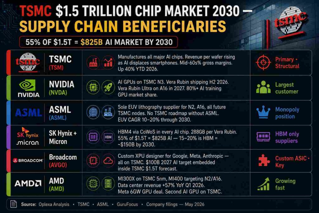
TSMC — The Best Risk-Adjusted Play on Its Own $1.5 Trillion Forecast
TSMC itself is the most structurally advantaged position in the TSMC $1.5 trillion chip market 2030 investment landscape. The logic: TSMC does not care which AI chip company wins. NVIDIA leads? TSMC makes NVIDIA chips. Google TPU displaces NVIDIA in inference? TSMC manufactures Google TPUs via Broadcom. Amazon Trainium 3 captures AWS workloads? TSMC makes Trainium chips. The TSMC $1.5 trillion chip market 2030 thesis does not require picking a winner — it only requires that AI infrastructure spending grows, which $700 billion in 2026 hyperscaler capex confirms.
TSM stock is up 40% in 2026. Gross margins expanded to 66.2% in Q1 — the highest in company history. Revenue intensity per wafer is rising as AI displaces smartphones in the product mix. TSMC is building capacity ahead of demand. The risk: TSM trades at 33.6x P/E versus a 5-year median of 22.78x, flagged at 38% overvalued by GF Value at the current price of ~$404. Investors evaluating the TSMC $1.5 trillion chip market 2030 story need to decide whether the structural AI demand shift justifies a sustained premium multiple.
Co-Packaged Optics — The Quiet Revolution Inside the $1.5 Trillion Forecast
Buried in the TSMC $1.5 trillion chip market 2030 roadmap is a technology that deserves more investor attention: Co-Packaged Optics (CPO) via TSMC’s COUPE platform. CPO replaces electrical signals between chips with pulses of light — delivering 50% lower power consumption and up to 90% reduction in AI data center latency for chip-to-chip communication.
TSMC confirmed CPO production samples go to customers in 2026. Partners include NVIDIA and Broadcom. The Silicon Photonics Industry Alliance (SiPhIA) that TSMC established is standardizing CPO integration across the AI chip ecosystem. For the TSMC $1.5 trillion chip market 2030 forecast, CPO opens a photonics revenue stream that expands TSMC’s addressable market beyond silicon — and it gives AI chip designers a path to higher performance that current electrical interconnect power budgets cannot support.
For enterprise AI teams, CPO is the hardware answer to the power crisis we covered in our AI Data Center Power Crisis 2026 analysis. Current generation chips require 100+ kW per rack and mandatory liquid cooling. CPO-enabled chips will reduce per-chip power density — but not before 2028 at scale. The TSMC $1.5 trillion chip market 2030 roadmap is how that ceiling eventually gets raised.
What the TSMC $1.5 Trillion Chip Market 2030 Means for Enterprise AI Strategy
The TSMC $1.5 trillion chip market 2030 forecast has practical implications for enterprise AI infrastructure teams — not just investors.
AI Chip Supply Gets Easier in 2027, Not 2026
TSMC’s nine fab phases in 2026 do not translate into chip availability in 2026. Semiconductor fabs take 18–24 months to build and equip. The capacity from 2026 construction comes online in 2027–2028. For enterprises procuring NVIDIA Vera Rubin or Google TPU v8 in H2 2026, supply stays constrained. The TSMC $1.5 trillion chip market 2030 is a 2027-and-beyond supply story. Procurement teams should plan for constrained availability through end of 2026 and improving conditions in 2027.
The Power and Cooling Problem Has a Roadmap Solution
Current AI chip generations require 100+ kW per rack. A16’s Super Power Rail and CPO-enabled optical interconnects — both in the TSMC $1.5 trillion chip market 2030 technology roadmap — will reduce per-chip power density for the 2027–2028 generation. This does not solve the 2026 power crisis. But it signals that the 100+ kW trajectory is not permanent — the TSMC $1.5 trillion chip market 2030 technology roadmap is specifically designed to break the power ceiling that currently constrains AI chip deployment economics.
TSMC Concentration Is Now Enterprise Operational Risk
With 55% of the TSMC $1.5 trillion chip market 2030 forecast concentrated in AI and HPC — and with TSMC manufacturing virtually every major AI accelerator platform — any TSMC supply disruption (earthquake, geopolitical escalation, yield crisis) affects every AI infrastructure platform simultaneously. Enterprise AI teams with material AI infrastructure dependencies should evaluate this concentration risk explicitly in their technology risk frameworks.
Conclusion — TSMC $1.5 Trillion Chip Market Is the Physical Foundation of Every AI Investment
The TSMC $1.5 trillion chip market 2030 forecast is not just a market size number. It is the physical foundation of every AI investment thesis in the semiconductor sector. NVIDIA’s $5 trillion valuation, Broadcom’s $100 billion 2027 AI revenue target, AMD’s data center growth, SK Hynix’s HBM expansion — all of it depends on TSMC’s ability to manufacture the chips that make AI run.
The TSMC $1.5 trillion chip market 2030 upward revision from $1 trillion signals three structural realities: AI chip demand is growing faster than even TSMC’s previous forecasts assumed, AI chips generate more revenue per wafer than any prior technology in TSMC’s history, and hyperscalers are not treating AI as a temporary cycle — they are committing $700 billion in capital against it in a single year.
The A16 delay creates near-term timing risk for 2027 chip generations. For enterprises, 2026 AI chip supply stays tight. For investors, TSM’s 38% premium to GF Value requires a view on whether structural AI demand sustains the elevated multiple. But for the decade-long TSMC $1.5 trillion chip market 2030 thesis — the demand is real, committed, and growing. The AI infrastructure buildout is the largest capital allocation event in technology history, and TSMC manufactures the hardware for all of it.
Frequently Asked Questions — TSMC $1.5 Trillion Chip Market 2030
What is TSMC’s semiconductor market forecast for 2030?
TSMC forecasts the global semiconductor market will exceed $1.5 trillion by 2030, raised 50% from its earlier estimate of $1 trillion. Announced at TSMC’s technology symposium on May 14, 2026. AI and HPC are expected to drive 55% of the $1.5 trillion market, smartphones 20%, and automotive 10%. TSMC is backing the TSMC $1.5 trillion chip market 2030 forecast with nine fab phases under construction in 2026 and 70% CAGR capacity growth for N2 and A16 through 2028.
Why did TSMC raise its 2030 chip market forecast to $1.5 trillion?
TSMC raised the TSMC $1.5 trillion chip market 2030 forecast because AI chip demand grew significantly faster than earlier projections. AI chips generate 4-6x more wafer revenue than smartphone chips. Hyperscalers have committed $700B+ in 2026 AI capex. CoWoS advanced packaging capacity is growing at 80% CAGR. CEO C.C. Wei calls AI demand structural rather than cyclical — and TSMC’s nine-phase 2026 construction program is built against committed customer purchase orders.
What is TSMC’s roadmap for 2026 and 2027?
TSMC’s current roadmap: N2 in production with 20+ tape-outs; Co-Packaged Optics samples in 2026 (50% power cut, 90% latency reduction); A16 delayed to 2027 volume production due to Super Power Rail complexity; N2U cost-efficient upgrade in 2028; A13 and A12 in 2029. N2 and A16 growing at 70% CAGR capacity through 2028 as part of the TSMC $1.5 trillion chip market 2030 buildout.
Why is TSMC A16 production delayed to 2027?
A16 volume production delayed from 2026 to 2027 due to complexity of integrating Super Power Rail (SPR) backside power delivery with nanosheet GAA transistors. The delay impacts NVIDIA Vera Rubin Ultra and Amazon Trainium 4. It does not affect 2026 chips — Vera Rubin and TPU v8 use N3 already in production. The A16 delay does not change the TSMC $1.5 trillion chip market 2030 structural forecast.
What is TSMC CoWoS packaging?
CoWoS (Chip-on-Wafer-on-Substrate) connects GPU dies, HBM memory, and networking chips into single AI accelerator packages. Essential for NVIDIA Blackwell/Vera Rubin, Google TPU v8, and Amazon Trainium 3. TSMC confirmed CoWoS yields topped 98% and capacity is growing at 80%+ CAGR through 2027. Expanding to 5.5x reticle size in 2026 and 9.5x by 2027 — critical for next-generation AI chip designs central to the TSMC $1.5 trillion chip market 2030 growth story.
Which stocks benefit from the TSMC $1.5 trillion chip market 2030 forecast?
Direct beneficiaries of TSMC $1.5 trillion chip market 2030: TSMC (TSM) — up 40% in 2026, mid-60s% gross margins; NVIDIA (NVDA) — AI GPUs on TSMC N3/A16; ASML (ASML) — monopoly EUV supplier for all advanced nodes; SK Hynix and Micron — HBM4 via CoWoS in every AI chip; Broadcom (AVGO) — custom XPUs on TSMC for Google, Meta, Anthropic; AMD (AMD) — MI series on TSMC, data center revenue +57% Q1 2026.
Related Oplexa Coverage:
- NVIDIA Vera Rubin GPU Guide — Uses TSMC N3 now, targets A16 for Ultra in 2027
- Broadcom AI Revenue 2026: $100B Target — All Broadcom XPUs on TSMC processes
- Amazon Trainium 3: $225B Chip Bet — TSMC 3nm, Trainium 4 targeting A16
- AI Data Center Power Crisis 2026 — A16 SPR + CPO are the hardware solution
- NVIDIA $5 Trillion Market Cap — Built on TSMC manufacturing dominance
- Custom ASIC Market 2026 — All custom ASICs on TSMC advanced nodes
📊 AI Chip Market Analysis & Forecast 2025–2035 — $1,499 — Full TSMC revenue model by node, AI chip demand scenarios, CoWoS capacity model, and 10-year investment thesis.
📊 NVIDIA Strategic Inflection Analysis 2025–2035 — $2,500 — TSMC A16 delay impact on Vera Rubin Ultra, NVIDIA revenue by node generation, 10-year GPU model.
📊 Custom ASIC Market 2026–2033 — $1,499 — Broadcom, Marvell, in-house AWS/Google on TSMC — market share projections, 7-year thesis.